
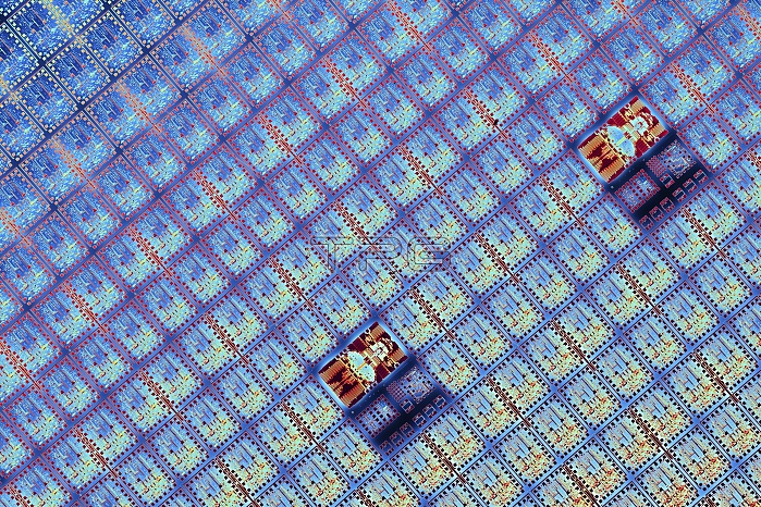
Computer enhanced image of a part of a semiconductor wafer. Wafers are divided up into blocks to make the integrated circuits ('chips') used in electronic devices. Hundreds of thousands of transistors can be fitted on a single chip and connected by conducting pathways. The complex pattern of circuits that comprises each chip is built-up in a series of processes involving masks, deposition of insulators and etchings. Finished chips are eventually diced from the wafer prior to packaging.
| px | px | dpi | = | cm | x | cm | = | MB |
Details
Creative#:
TPG09626072
Source:
達志影像
Authorization Type:
RF
Release Information:
須由TPG 完整授權
Model Release:
no
Property Release:
no
Right to Privacy:
No
Same folder images:
 Loading